by MBF Admin | Sep 14, 2020 | 2D materials, Aerospace, AGM, Angstron Materials, Audio, Development, Graphene applications, Graphenea, Investment, Products, Research, Transistors
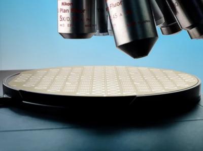
Graphenea recently announced that its graphene foundry service (GFAB), launched in 2019, will be getting an upgrade. Graphenea Foundry said that it will start a Multi-Project Wafer run service from January 2021, and it is currently speaking with customers interested...
by MBF Admin | Apr 24, 2020 | 2D materials, Aerospace, AGM, Angstron Materials, Audio, Development, Graphene applications, Graphenea, Investment, Products, Research, Technical / Research, Transistors
Graphenea has announced the successful completion of project G4SEMI, funded by the European Commission SME Instrument.The project, which lasted two years, aimed at integrating graphene into CMOS semiconductor workflows. The business goal was to create added value...
by MBF Admin | Mar 24, 2020 | 2D materials, Aerospace, AGM, Angstron Materials, Audio, Development, Directa Plus, Graphene Sensors, Graphene videos, Graphene-Info, Graphenea, Investment, Medicine, Products, Research, Rice University
As researchers and companies all over the world set out to battle the Coronavirus pandemic, many are revisiting graphene as a material with potential for helping to win this fight. The reasons for such potential could be found in graphene’s known...
by MBF Admin | Mar 24, 2020 | 2D materials, Aerospace, AGM, Angstron Materials, Audio, Development, Graphenea, Investment, Medicine, Products, Research
With the emergence of the Covid-19 virus and its global threat, Graphenea initiated several steps to try and help those trying to combat this crisis. On March 16th, Graphenea approached all those performing research on treatment and diagnosis of Covid-19, to offer...
by MBF Admin | Dec 1, 2019 | 2D materials, Aerospace, AGM, Angstron Materials, Audio, CVD, Development, Electronics, Graphene applications, Graphenea, Investment, Membranes, Products, Research
Graphenea has announced the launch of a new product – highly flat monolayer graphene. The graphene is grown by CVD on copper thin film on a 2” sapphire substrate. With extremely low roughness that is less than 4 nm, this new product is targeted at applications in...
by MBF Admin | Mar 28, 2019 | 2D materials, Aerospace, AGM, Angstron Materials, Audio, Development, Electronics, Graphene applications, Graphenea, Investment, Products, Research, Technical / Research
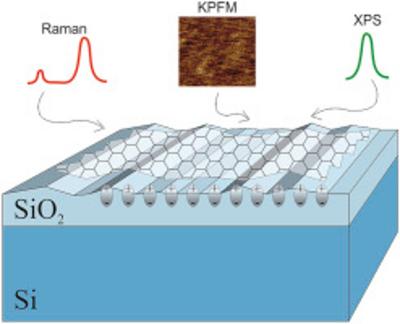
Due to graphene’s 2D geometry, most of the device applications require graphene to be partially or fully supported by a substrate, which is typically silicon dioxide (SiO2). An important example of a typical graphene structure on SiO2 is the graphene field...